![]() ;
;
![]() ;
;
![]() ;
;
![]() ;
Updated in
;
Updated in
![]() 2024 :
2024 :
![]() June :
June :
![]() 25th
(Tuesday) : Network Topology ;
25th
(Tuesday) : Network Topology ;
![]() ;
;
![]() ;
;
![]() ;
;
![]() ;
Updated on
;
Updated on
![]() 25 :
25 :
![]() 6 :
6 :
![]() 2024 :
Transistor ;
2024 :
Transistor ;
2 nm; 3 nm; e.g.
graphene is a good keyword to realize & understand ... ;
(![]() 2 nm,
2 nm, ![]() 3 nm),
also see: Action;
IoT;
n Computer;
Network Topology;
Processor;
Transistor;
3 nm),
also see: Action;
IoT;
n Computer;
Network Topology;
Processor;
Transistor;
(![]() TFT,
TFT,
![]() TFT,
TFT,
![]() TFT,
TFT,
![]() TFT), also see: Computers;
TFT), also see: Computers;
 |
L Using | Injector | To Be | Parallel | IC28 | ; | |||
 |
L | Prior | To | Parallel | IC28 | ; | |||
 |
98 | _LBZCS | _Window | ; | |||||
 |
98 | _LTZCS | _Window | ; | |||||
 |
98 | _RBZCS | _Window | ; | |||||
 |
98 | _RTZCS | _Window | ; | |||||
for 21st century & beyond, e.g. 99% transparency plastic computer, e.g. 99% transparency plastic computing, e.g. 99% transparency plastic smart phone, ... ;
think THAT 6 Sheets of paper are approx. 1 mm thick, and those 6 Sheets of paper are at 1 location, and those 6 Sheets of paper obey iroColourWaveForm ... ; after defining Origin of Sound, kuru kuru WHILE (dimensional, directional, logical, numerological, structural), transistors alike characteristics are ... , we've 99% transparency plastic computer, 99% transparency plastic computing, 99% transparency plastic smart phone, ... ; Remark: to be in market, too early in the year (2563, 2020);
because of
DEE (Dark Energy
Engineering),
![]() wareware We've been using Gravity
Dimension Computer, and PHYSICS, law 123,
lights can be using NOT ONLY for pressure, BUT ALSO for sound, so
THAT 99% transparency plastic ... instead of superconducting (impedance in the
transmission line, kinetic inductance, qubit) ... ; for easy and simple
understanding, also see:
wareware We've been using Gravity
Dimension Computer, and PHYSICS, law 123,
lights can be using NOT ONLY for pressure, BUT ALSO for sound, so
THAT 99% transparency plastic ... instead of superconducting (impedance in the
transmission line, kinetic inductance, qubit) ... ; for easy and simple
understanding, also see:
 ,
,
 ;
;
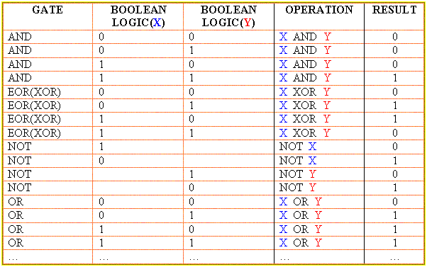
In common, since 1950s, making software logic gates deployable, hardware chips are made of transistors [transistor is semiconductor], and also known as TRAN s f e r Re SISTER; Vacuum tubes were used to do calculation of logic but slower and higher energy consumption; For faster processing speed and lower energy consumption, transistors have been used; Transistors have been replaced vacuum tubes for a half century; Theoretically, basic logical calculations are based on Boolean Logic; Gate is made of transistors; Gates' input/output values in Truth Table have been used to calculate both advance logic and basic Boolean logic;
For novice system programmers: Apply Syntax vs. Semantic concept between Gate and Transistor, and notice that gates are more likely to be in software usage, and transistors are more likely to be in hardware usage, and study of gate vs. transistor should be in materials engineering and chemical/physical research development because material makes transistor, transistor makes logic gate;
Also see: NEC and NEC Electronics; Semiconductor;
Transistors Usages: Transistor (*RAM transistors) (Repeated transistors) (ROM transistors) (Unique transistors non-repeated) (...);
3D Transistor a.k.a. S-R ACT;
a-S i, Amorphous Silicon TFT fabrication; Ash i n g;
Band
gap
![]() ;
Base
Old usage; Behavior(
(Alpha cutoff) (Gain bandwidth product) (...));
B J T, Bipolar
Junction Transistor; Bonding;
BOX layer
SOI;
;
Base
Old usage; Behavior(
(Alpha cutoff) (Gain bandwidth product) (...));
B J T, Bipolar
Junction Transistor; Bonding;
BOX layer
SOI;
![]() basicLogic1;
basicLogic1;
![]() basicLogic2;
basicLogic2;
![]() basicLogic3;
basicLogic3;
![]() basicLogic4;
basicLogic4;
![]() basicLogic5;
basicLogic5;
![]() basicLogic6;
basicLogic6;
![]() basicLogic7;
basicLogic7;
![]() basicLogic8; (Maroon Color (A),
Red Color (B)) As Input, And
Then, (((A (0), B (0)) output 1), ((A (0), B (1)) output 0), ((A (1), B (0))
output 0), ((A (1), B (1)) output 1)), a.k.a. Exclusive NOR, a.k.a. X NOR,
a.k.a. EX NOR;
basicLogic8; (Maroon Color (A),
Red Color (B)) As Input, And
Then, (((A (0), B (0)) output 1), ((A (0), B (1)) output 0), ((A (1), B (0))
output 0), ((A (1), B (1)) output 1)), a.k.a. Exclusive NOR, a.k.a. X NOR,
a.k.a. EX NOR;
Carbon Nano tube transistor NEC: development stage In 2005; Carrier mobility [better portability]; Caulking; (Cell layout (DIFF) (MET-1) (MET-2) (NWELL wells = tubs where n-type substrate creates p-well, p-type substrate creates n-well) (P+) (POLY) (...)); (Characteristic (DC) (Function) (...) ); Characteristics in 2D, 3D, 4D, ... where information flows how; CMOS; (C M OS FE T phase controlled ((N FE T gate electrode) (P FE T gate electrode)) (...)); (Coating (Photo-resist) () ); Collector Old usage;
![]()
![]()
![]() Plus || Minus, a.k.a.
Plus || Minus, a.k.a.
![]() Plus Or Minus; Also see:
Inductance;
Plus Or Minus; Also see:
Inductance;
D,
Drain
FET electrode;
Decoupling; Depletion; (Deposition (CVD, Chemical
Vapor
Deposition) (Sputtering method) (...) );
Dicing; Direct tunneling current; (Distortion compensation
![]() (D P D,
Digital Pre-Distortion));
Drain current [MOS
transistor's drain current]; Drain voltage;
(D P D,
Digital Pre-Distortion));
Drain current [MOS
transistor's drain current]; Drain voltage;
Emitter Old usage; Encapsulation; E pi tax i a l layer; (Etching (Dry etched by gas Plasma etch) (Wet etched by liquid chemical Chemical etch; HF Acid etch; ) (...) );
FD SO I, Fully Depleted Silicon On Insulator transistor double gate in 2004 for So C; (FE T (HE MT) (J FE T, Junction Field Effect Transistor) (M OS FE T, Metal Oxide Semiconductor FE T)); (Film (Field-oxide film, insulation layer) (Metallic film) (Ni film) (Nitride film) (Oxide film) (Poly silicon film) (...) );
G,
Gate
FET electrode;
Gain; (Gate (MOS-transistor)
(Poly-Si/high-k) (Poly-Si/SiO2) (...) );
(Gate depletion (Poly-Si) (...) );
(Gate dielectric![]() (high-k) (H f S i ON) (low-k
low dielectric constant material [65nm
in 2004]
(high-k) (H f S i ON) (low-k
low dielectric constant material [65nm
in 2004]
![]() )
(...) ); (Gate electrode (Metal) (...)
); Gate leakage [the lower the gate leakage, the better the
transistor is]; Gold fine wire;
)
(...) ); (Gate electrode (Metal) (...)
); Gate leakage [the lower the gate leakage, the better the
transistor is]; Gold fine wire;
(HE MT (Al N) (Ga N) (S i C) (...));
IFF using (electricity
![]() OR light
beam) meta material
... ; Ingot;
(Inspection (Final inspection) (Sampling inspection) (Wafer inspection) (...)
); Ion implantation;
iroLED; Island;
OR light
beam) meta material
... ; Ingot;
(Inspection (Final inspection) (Sampling inspection) (Wafer inspection) (...)
); Ion implantation;
iroLED; Island;
(Layer (Cover layer, after metallization) (Diffusion (p-type diffusion = n-type transistor) (...) ) (Ga As layer) (insulation layer, also known as gate oxide) (SiO2 layer) (...) ); (Layout (Cell layout) (Mask layout) (...)); Lead frame; Leak current Back-gate bias must apply; Also see: Gate leakage; Library One library may contains hundreds of cells such as flip-flops, gates, inverters, latches, ... ; (Logic circuit design (CAD) (IC function) (Layout design) (Mask pattern) (...) ); LOP transitor, Low Operation Power [In 2004, micro-amp, OR nano-amp are recommended]; LSI If signal delays because of line to line F, low-k is recommended to reduce capacitance; Also see: Hitachi; L S TP, Low Standby Power;
ME S FE T, Metal Semiconductor Field Effect Transistor; Metal gate a part of SO I transistor; Metallization; Modular structure; Mounting;
Ni, Nickel; N MOS;
Operating speed;
p-S i, Poly Silicon T F T fabrication; Patterning; Photo-mask; Pinch off; PM OS; Poly-S i, Polycrystalline Silicon; Poly cell = Standard cell; Probe r; (Process procedure (Full s i l i c id at i on annealing) (Micro-fabrication (Transistors) (Diodes)) (Wafer fabrication) (...) ); (Processing (BE) (FE) );
(Ratio of composition (Ni/S i) (...) ); R CAT, Recess Channel Array Transistor, 50nm, Samsung, 2006;
S, Source FE T electrode; Saturation state; S i l i c id at i on; Silver paste resin; SoC, System-on-Chip; SOG, Sea of Gates; SOI, Silicon On Insulator; SO I transistor Tunable threshold V tech = Metal gate + variable threshold voltage by ion implantation, Sputtering method; (Stepper (UV photo-mask) (...)); (Stripping (Photo-resist) (...) ); Sub-threshold current;
Tester; TFT, Thin-film transistor; Trans-conductance J FE T Analog dynamic mutual conductance;
Ultraviolet beam radiation etches microscopic transistors onto wafer, WHERE wafer is made of silicon, therefore, silicon transistors ... , therefore to categorize various types and levels;
V th, Threshold voltage one of the most important parameters of CMOS;
(Wafer (Wafer fabrication (Lithography method) (...) ) (Wafer inspection, where human logic becomes the most important also see Tester and Probe r) (...) );
 X NOR; Also
see: Battery;
X NOR; Also
see: Battery;
Basic understanding of transistors' functions are shown below:
| N P N, PNP Current Flow: from Emitter to Collector (without modulating) | |||||||
| N | P | N | |||||
| Emitter | _ | + | _ | Collector | |||
| Base | |||||||
| P | N | P | |||||
| Emitter | + | _ | + | Collector | |||
| Base | |||||||
| FET | |||||||
| + | |||||||
| _ | _ | ||||||
| Source | Drain | ||||||
| + | |||||||
| Gate | |||||||
| FE T Current Flow: from Source to Drain (with modulating / electric field at Gate) | |||||||
Also see: Basic gates [ *gate: ]; Symbolic schematic gates;
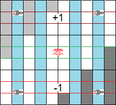
Basic understanding of Truth Table is shown below:
![]()
![]()
![]()
![]()
![]()
![]()
![]()
![]()
![]()
![]() NAND
gate
NAND
gate
![]() NAND
element;
NAND
element;
![]()
![]()
![]()
![]()
![]() NAND operation
NAND operation
![]() non-conjunction, NOT-BOTH operation;
non-conjunction, NOT-BOTH operation;
![]()
![]()
![]() NAND
NAND
![]() (gate, circuit) not -
and;
(gate, circuit) not -
and;
For Monbusho level developers only: with brunching factor 2 [larger the factor number, harder the logic], reversely engineer from leaf depths [deeper the tree depth, longer the path] to root, use of A, B, C, D, E, ... , and fully distributed connection ((N (N-1)) / 2 ), and make advance nama logic for Asimo Ukon and later ... ;
|
|
|
|
|
|